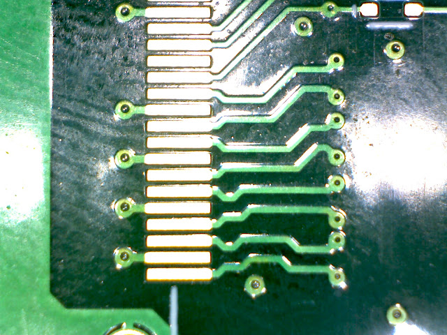
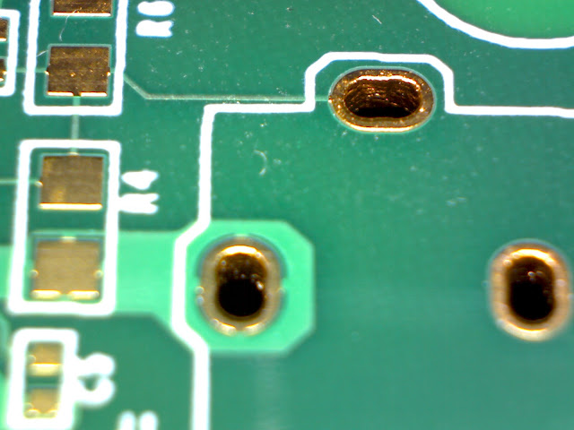
Tonight after yet another hiccup by DHL I've finally received a second revision of my Artix board. This time to my eye the boards came out with even better quality. Judge for yourself.
The only visible change in revision 2 is presence of termination resistor under DDR3 module for the clock line.
Can't wait to assemble the board to see if it will actually work!
 |
| Scan of the board's front side |
 |
| Scan of the board's back side |
 |
| FPGA footprint |
 |
| FPGA footprint |
 |
| DDR3 module footprint |
 |
| DDR3 module footprint |
 |
| DDR3 module footprint |
 |
| FTDI FT601 USB 3.0 to FIFO bridge (0.4 mm pitch QFN) |
 |
| FTDI FT601 USB 3.0 to FIFO bridge (0.4 mm pitch QFN) |
 |
| Main PMIC (TI's TPS65400, 0.5 mm pitch QFN) |
 |
| Main PMIC (TI's TPS65400, 0.5 mm pitch QFN) |
 |
| 12 to 5 V DC-DC converter (TI's TLV62130, 0.5 mm pitch QFN) |
 |
| 12 to 5 V DC-DC converter (TI's TLV62130, 0.5 mm pitch QFN) |
 |
| 0.5 mm pitch FRC connector (left), 0804 termination resistor arrays (right) |
 |
| 0.5 mm pitch FRC connector (left), 0804 termination resistor arrays (right) |
 |
| HDMI connector footprint (diff pairs are visible) |
 |
| HDMI connector footprint (diff pairs are visible) |
 |
| SPI Flash footprint |
 |
| Exposed backplate under main PMIC IC |
 |
| Exposed backplate under 12-5V DC-DC converter |
 |
| Exposed backplate under 12-5V DC-DC converter |
 |
| Back side of DDR3 module with new footprint for termination resistor |
 |
| Decoupling capacitors under FPGA (0201 and 0402 footprints are visible) |
 |
| Decoupling capacitors under FPGA (0201 and 0402 footprints are visible) |
 |
| Microsection |
 |
| Microsection |
 |
| Microphoto showing thru-hole plating |
 |
| Microphoto showing thru-hole plating |
 |
| Microphoto showing thru-hole plating |
Can't wait to assemble the board to see if it will actually work!
No comments:
Post a Comment